PCB Design for Manufacturing Guidelines: What Your Design Files Need Before They Go to a Factory
TL;DR
- Gerbers alone are not enough for production readiness
- PCB manufacturability depends on layout, BOM, assembly, and test coverage
- Test access must be designed in early
- BOM risk is part of DFM, not a separate task
- A proper pre-submission checklist can save months of rework
Too many founders make the same expensive mistake: they send Gerbers to a factory, hear “no problem,” approve a quote, and assume they are ready. Then the first boards arrive with solder bridging, inaccessible test points, unstable components, or assembly issues that make scaling impossible.
That failure usually starts in the design files and not on the factory floor.
Printed Circuit Board design for manufacturing (PCB DFM) is the process of designing a circuit board so it can be fabricated, assembled, tested, and scaled without avoidable yield loss, quality failures, or supply chain surprises.
For electronics founders, PCB DFM is one of the highest-leverage risk reduction steps in the entire launch. Morpho treats it as a structured engineering discipline. We help funded founders building electronics products, testing PCB designs, protect BOM stability through our Component Control Method (CCM), and build manufacturing systems that hold up under real production conditions.
What Is PCB DFM?
PCB DFM means designing your board so the factory can fabricate and assemble it consistently, without hidden yield, quality, or rework risk.
A manufacturable PCB is not just electrically functional. It must also be:
- easy to fabricate
- easy to assemble
- easy to inspect
- easy to test
- resilient to component supply risk
This matters because prototype success is a weak signal.
A hand-built EVT board that works on the bench can still fail in volume because of:
- trace spacing too tight for yield
- pads that tombstone components
- poor connector clearances
- inaccessible test points
- fragile BOM choices

The Real Cost of Skipping PCB DFM
When PCB DFM is treated as an afterthought, problems show up late and expensively.
Common failure patterns:
- boards fail AOI due to pad geometry
- solder bridges from poor spacing
- warped boards from bad stack-up choices
- high rework rates during SMT assembly
- field failures due to weak connectors or thermal issues
These are not factory mistakes. They are usually design-to-manufacturing failures.
A strong PCB DFM review protects:
- yield
- timeline
- margin
- customer trust
Core PCB DFM Rules That Actually Matter

1. Trace Width and Spacing
Your trace rules must match:
- current requirements
- impedance needs
- fab process limits
Key checks:
- minimum trace width aligns with fab capability
- differential pairs are controlled
- high-current paths are sized safely
Too-tight spacing increases defect risk and lowers yield.
2. Via Design and Drill Constraints
Vias affect both reliability and cost.
Check:
- drill size compatibility
- annular ring margins
- via-in-pad risk
- aspect ratio limits
Poor via design creates fabrication and assembly issues fast.
3. Component Placement and Assembly Access
Placement should support assembly, inspection, and serviceability.
Key rules:
- maintain keepout zones
- align polarized components consistently
- allow pick-and-place access
- protect heat-sensitive parts
A board that is electrically clean but hard to assemble is not production ready.
4. Solder Mask, Paste, and Silkscreen
Your board needs clear manufacturing communication.
Review:
- solder mask clearances
- paste aperture sizing
- reference designator legibility
- polarity markings
This reduces assembly errors and rework.
5. Panelization and Board Handling
Factories build panels, not single boards.
Check:
- breakaway tabs / V-score suitability
- fiducial placement
- tooling hole access
- panel rigidity
Ignoring panelization early often creates avoidable NPI delays.
6. IPC Class and Quality Standards
Align your board to the right manufacturing standard.
For many products:
- IPC Class 2 fits consumer / commercial use
- IPC Class 3 may be needed for high-reliability use cases
Your design intent should match your quality target.
BOM Considerations for PCB Manufacturing
PCB DFM is not complete without BOM discipline. Your board can be perfectly laid out and still fail because of supply chain risk. You need to know that if you want to scale in electronics manufacturing.
Key BOM DFM checks:
- avoid EOL / NRND components
- avoid single-source dependencies
- validate alternates early
- confirm package availability
- verify footprint matches schematic and layout
Non-standard packages create hidden launch risk.
Morpho’s CCM protects founders from silent substitutions and BOM instability that destroy margins later.
Test Coverage Is a DFM Issue, Not a Postscript
Most founders think about testing too late.
That is a major mistake.
Your PCB should be designed for the test method your manufacturing partner will actually use.
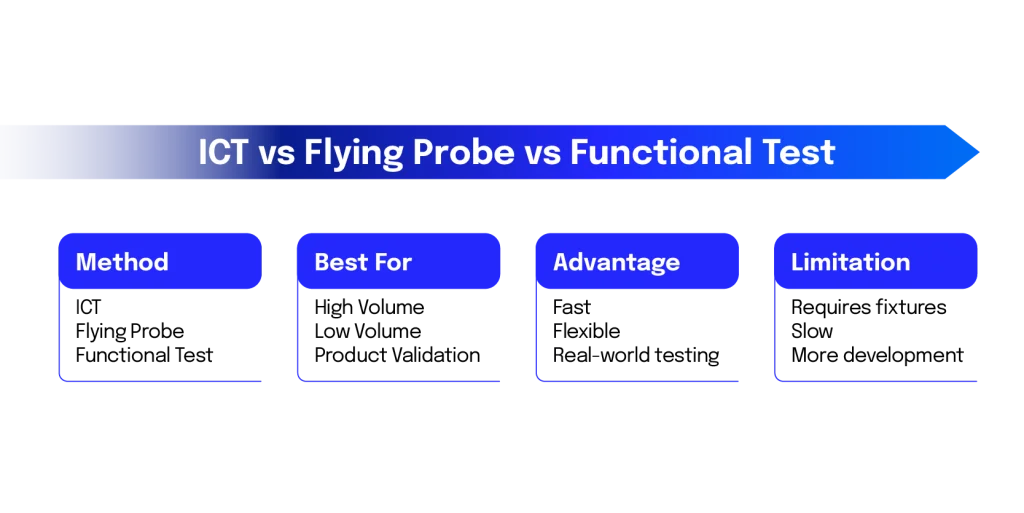
Common test methods:
ICT (In-Circuit Test):
- best for volume
- requires test point access
Flying Probe:
- flexible for low volume
- slower, less scalable
Functional Test:
- validates real product behavior
- should be planned into firmware / hardware flow
PCB DFM should verify:
- test point accessibility
- fixture compatibility
- debug interfaces
- programming access
- power-up validation flow
A board that cannot be tested efficiently becomes expensive to scale. If you want to dive deeper into rapid prototyping for electronics, check here.
Evermix: Why PCB DFM Matters in Real Products
Evermix is a DJ streaming and recording hardware product with audio-specific PCB requirements.
Audio electronics are especially sensitive to:
- signal integrity
- grounding strategy
- component noise
- connector durability
Evermix is a strong example of why PCB DFM cannot be reduced to passing ERC and DRC checks.
To manufacture reliably, products like this require:
- layout decisions that protect yield
- component sourcing discipline
- production test planning
- packaging validation
Morpho helps founders solve these issues before production.
PCB DFM Guidelines Checklist: Verify These 12 Things Before Sending Gerbers

Layout and Fabrication
1. Trace width / spacing match fab capability
2. Via sizes and drill rules are validated
3. Stack-up and copper balance are reviewed
4. Keepout zones and clearances are clean
Assembly
5. Component orientation supports assembly speed
6. SMT spacing supports reflow yield
7. Solder mask / paste layers are verified
8. Panelization plan is define
BOM and Supply
9. No EOL / high-risk components remain
10. Alternate parts are identified
Test and Validation
11. Test points support ICT / flying probe / debug
12. Programming / functional test flow is planned
This checklist should happen before RFQ—not after first articles.

Ready to Really Understand Your PCB Before Production?
If you are preparing to send PCB files to a factory, this is the point where small oversights become expensive launch problems.
Morpho helps founders building electronics products pressure-test layouts, protect BOM stability, and build production systems that scale.
Book a strategy call before you send your files. It is far cheaper to fix a board now than after your first failed production run.
What is a Discovery Call?
- A free and no-commitment 30-minute session to assess your product, understand Morpho’s process, and map your next steps.
- We’ll validate if your design is manufacturable and compliant.
- You’ll gain guidance on risks, timelines, and our proven premium-build process.
Book a Discovery Call and learn how Morpho can help you move confidently from idea to production.
FAQ (2026)
What are PCB design for manufacturing guidelines?
PCB DFM guidelines are design rules and process checks that ensure a board can be fabricated, assembled, tested, and scaled reliably.
What files do I need for PCB manufacturing?
At minimum: Gerbers, drill files, pick-and-place data, BOM, assembly drawings, stack-up details, and test requirements.
How do I check if my PCB is manufacturable?
Review layout rules, assembly constraints, BOM risk, and test coverage with a manufacturing engineering partner before sending files.
Author & Last updated
MorphoMFG Engineering Team — Expert, bold, people-first guidance for hardware founders.
- Last updated:
Table of Contents